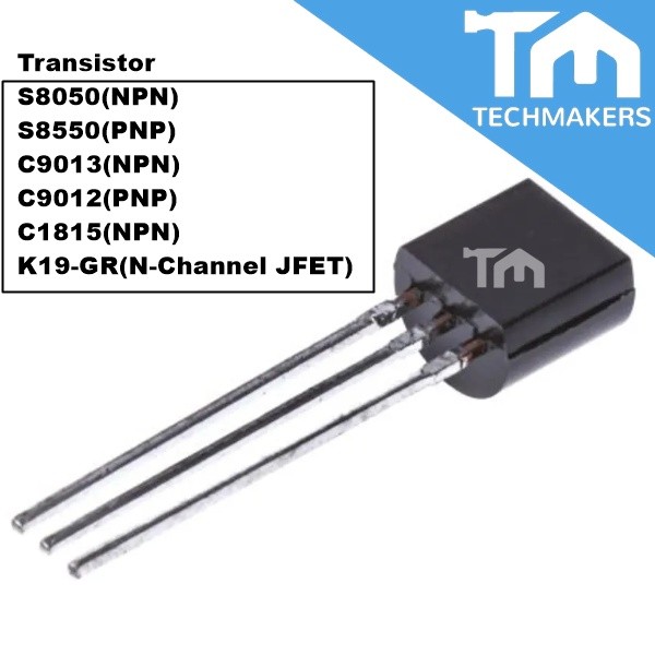
1pc of S8050/ S8550/ C9013/ C9012/ C1815/ K19-GR Transistor TO-92 Small Signal Amplifier0.5A/40V
has variants
Home Appliances › Electrical Circuitry & Parts › Others
id 4419423387first seen 29 Apr 2026, 10:45 pmlast seen 2mo agodetail 2mo ago
Sold (Shopee)
386
tracked: not enough snapshots yetlatest 2mo ago
Latest price
RM0.40
Rating
5.00 ★
Variants
6
Sold count history
last 90 daysPrice range history
last 90 daysVariants
6 active| Variant | Price | Δ | Stock | First seen | Updated |
|---|---|---|---|---|---|
C1815 | RM0.60 | RM0.00 | in stock | 2mo ago | 2mo ago |
C9012 | RM0.40 | RM0.00 | in stock | 2mo ago | 2mo ago |
C9013 | RM0.40 | RM0.00 | in stock | 2mo ago | 2mo ago |
K19-GR | RM1.50 | RM0.00 | in stock | 2mo ago | 2mo ago |
S8050 ( NPN) | RM0.40 | RM0.00 | in stock | 2mo ago | 2mo ago |
S8550 (PNP) | RM0.40 | RM0.00 | in stock | 2mo ago | 2mo ago |
Variant price history
last 365 days · sampled by weeklyscan:fullS8050 ( NPN)S8550 (PNP)C9013C9012C1815K19-GR
Description
Desciption: S8550 is a general purpose transistor therefore you can use it at the output of your audio amplifier circuits to amplify the output audio signal to 1 watt, for example it can used in electronic doorbell circuits, mp3 audio amplifiers and in the output of buzzer circuits. Specification: - Type Designator: S8550 - Polarity: PNP - Package: TO-92 - Maximum Collector Power Dissipation (Pc): 0.3W - Maximum Collector-Base Voltage (Vcb): 40V - Maximum Collector-Emitter Voltage (Vce): 25V - Maximum Emitter-Base Voltage (Vbe): 5V - Maximum Collector Current (Ic max): 0.5A - Maximum Operation Junction Temperature (Tj): 150°C - Transition Frequency (ft): 150 MHz - Foward Current Transfer Ratio (hFE), Min: 120 Description: S8050 is a NPN transistor which has a maximum gain value of 400; this value determines the amplification capacity of the transistor normally S8050. Since it is very high it is normally used for amplification purposes. However at a normal operating collector current the typical value of gain will be 110. The maximum amount of current that could flow through the Collector pin is 700mA, hence we cannot drive loads that consume more than 700mA using this transistor. To bias a transistor we have to supply current to base pin, this current (IB) should be limited to 5mA. When this transistor is fully biased then it can allow a maximum of 700mA to flow across the collector and emitter. This stage is called Saturation Region and the typical voltage allowed across the Collector-Emitter (VCE) or Collector-Base (VCB) could be 20V and 30V respectively. When base current is removed the transistor becomes fully off, this stage is called as the Cut-off Region. Specification: Low Voltage, High Current NPN Transistor Small Signal Transistor Maximum Power: 2 Watts Maximum DC Current Gain (hFE): 400 Continuous Collector current (IC) : 700mA Base- Emitter Voltage (VBE) :5V Collector-Emitter Voltage (VCE) : 20V Collector-Base Voltage (VCB) : 30V Package: TO-92 Design for Class B audio amplifier and general purpose applications